
BDS Tech is headquartered in Hangzhou and co-established a joint laboratory in Beijing with the Institute of Computing Technology, Chinese Academy of Sciences (ICT, CAS). Our core R&D team comes from Huawei HiSilicon and ICT, CAS, bringing deep expertise in chip and system engineering.
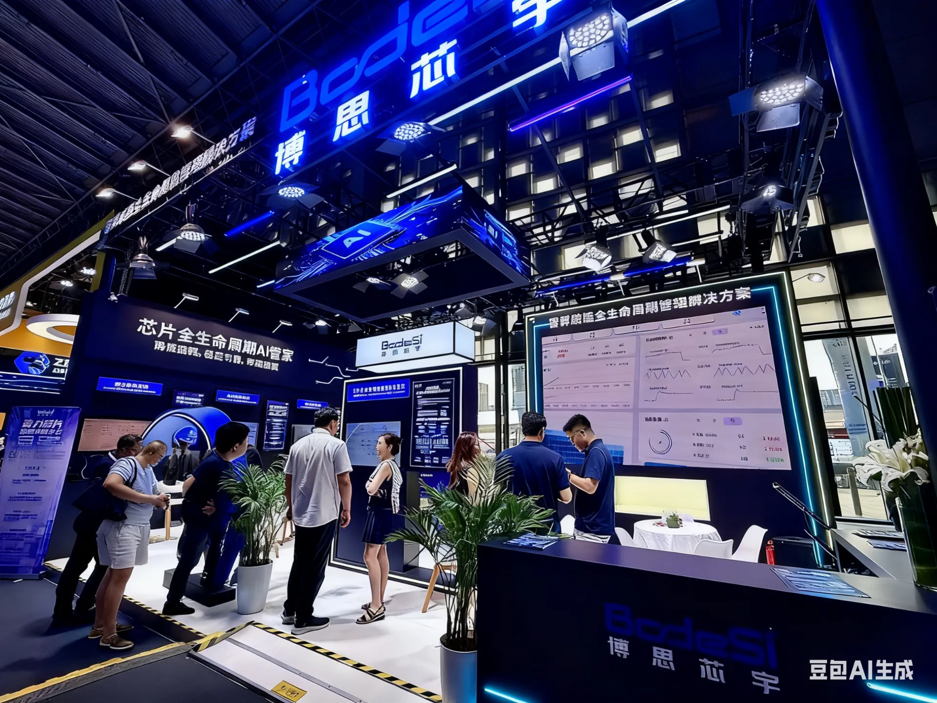
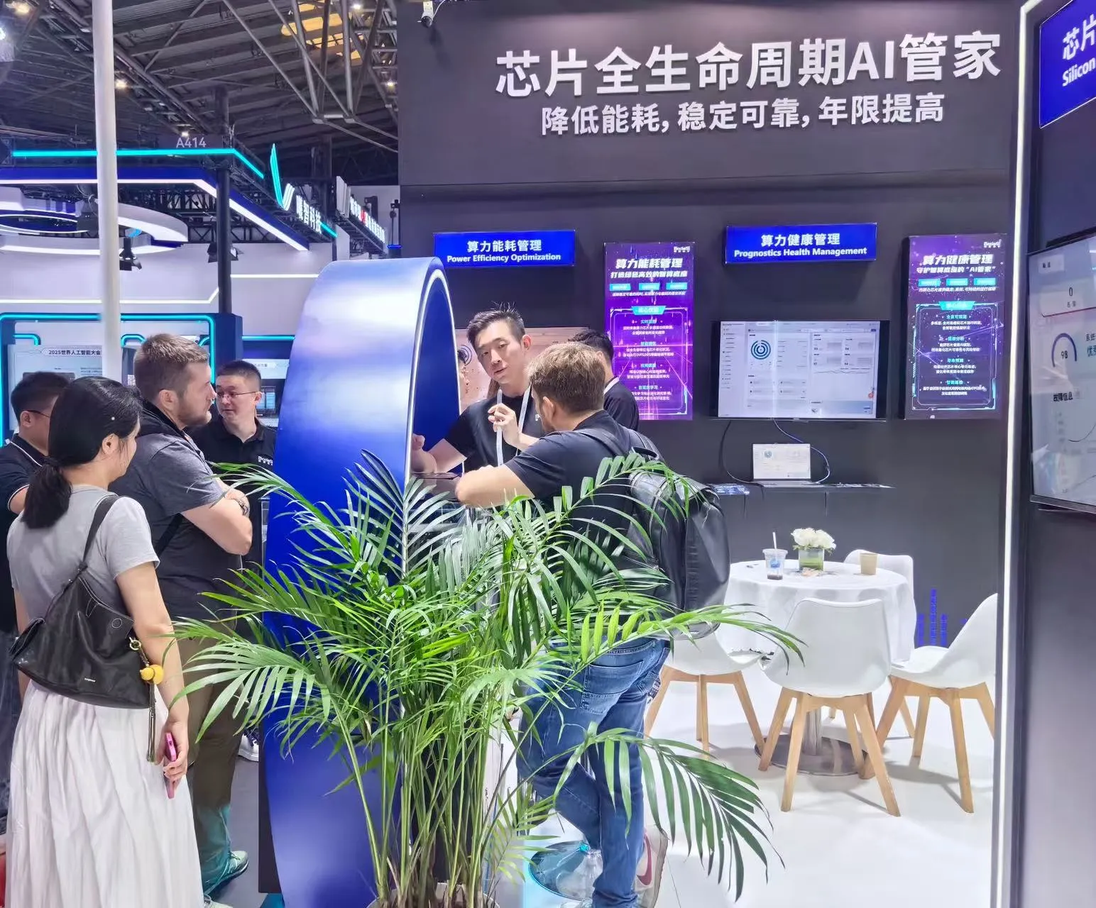
With Silicon Lifecycle Management (SLM) at the core, we build data-driven solutions for AI infrastructure—covering chip- and cluster-level monitoring, analytics, and optimization. Powered by our self-developed chip health models, we create a standardized framework for managing AI compute chips across their full lifecycle. Today, we primarily serve AI data centers and enterprise compute clusters with a chip-health-aware management platform, focused on reducing chip energy consumption, improving cluster reliability, and enhancing overall efficiency while lowering operating cost.
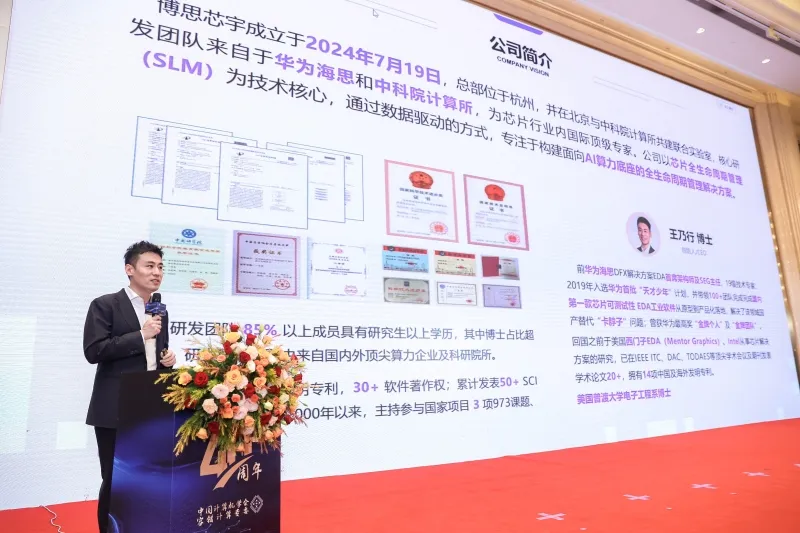
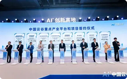
Hangzhou BDS Technology Co., Ltd. was established in July 2024 and is located in the Future Science and Technology Center of Yuhang District, Hangzhou. It is a key project supported by the Yuhang District government and has landed in Yuhang. The founder, Dr. Wang Naixing, was awarded the title of Yuhang District Innovation and Entrepreneurship Talent. In October 2024, the company successfully completed an angel round financing of tens of thousands of yuan, jointly invested by Zhejiang Huarui Investment and Qidi Star Venture Capital, laying a solid foundation for the rapid development of the enterprise. In October 2024, Hangzhou BDS Technology Co., Ltd. was selected as one of the first key projects to settle in; Al Innovation Highland "- China Cloud Valley, further promoting the layout and growth of enterprises in the field of artificial intelligence computing infrastructure.


The company currently has two major office bases in Hangzhou and Beijing. Hangzhou serves as the headquarters, carrying out overall corporate functions, while Beijing focuses on the core work of the joint laboratory with Bosenxin and the Chinese Academy of Sciences. To further advance the company's strategic deployment in the Yangtze River Delta region and even nationwide in the field of artificial intelligence, the company plans to officially enter the Shanghai Changyang Chuanggu Qidi Star High-Quality Incubator Headquarters Building this year. Together with Qidi Star, we will jointly build an incubator edge data center, continuously expanding market reach and innovation space.
Former Chief Architect and SEG Director of Huawei HiSilicon DFX Solution EDA, a 19th-level technical expert; selected in 2019 for Huawei's first batch of the "Genius Youth" program, leading a 100+ team to complete the development and productization of China's first chip testability EDA industrial software from prototype to market launch, solving the domestic substitution "bottleneck" issue in this field; recipient of Huawei's highest awards, including "Gold Medal Individual" and "Gold Medal Team".
Prior to returning to China, engaged in chip solution research at Siemens EDA (Mentor Graphics) and Intel in the United States. Has published 20+ academic papers in top-tier academic conferences and journals such as IEEE ITC, DAC, and TODAES, and holds 11 Chinese and international invention patents.
Ph.D. in Electrical Engineering from the University of Maryland, USA
Assess and monitor the health status, performance, etc. of the graphics card
Online analysis and intelligent optimization to reduce computational energy consumption and extend chip lifespan
Chip health monitoring and early warning to ensure hardware is maintainable and manageable throughout its entire lifecycle.
Stepwise utilization, allowing computing power cards to be optimally applied at different stages, rather than being phased out too early.
Centered on full lifecycle management of chips, providing one-stop service for intelligent computing base management platform
Contact Us